Can You Upload Plc Specs Into Multisim
Tutorial: Creating and Exporting a PLD Schematic
Multisim Help
Edition Date: February 2017
Part Number: 375482B-01
View Product Info
DOWNLOAD (Windows Simply)
This tutorial demonstrates how to create and simulate a PLD schematic.
To complete this tutorial, y'all volition need:
- The NI Digital Electronics FPGA Board and its driver.
- A supported version of Xilinx ISE.
When you install Xilinx, select the Become Costless ISE WebPack License option.
The process described here can as well be used to target whatever of these Digilent boards:
- Basys FPGA Board.
- Basys 2 FPGA Lath.
- Nexys 2 FPGA Board.
- Nexys 3 FPGA Lath.
- Nexys 4 FPGA Board.
- NI Digital Systems Development Board.
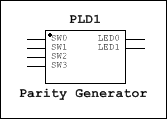
You volition create the post-obit simple 4-bit parity generator:

When consummate, PLD1 will comprise the following logic:
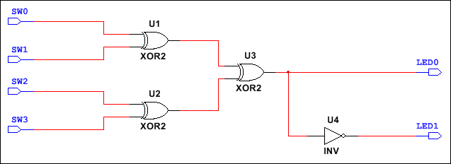
 The completed design is found at
 ...\samples\PLD Sample Circuits\ParityGenerator.
You will so export the PLD device to the National Instruments Digital Electronics FPGA Board, which includes the Xilinx Spartan 3E FPGA.
Creating the design
Consummate the following steps:
- Select File»New.
- Select Blank and click Create.
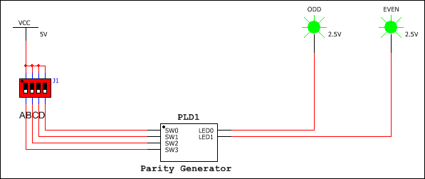
- Place VCC, J1 and the probes.
- Change the Reference Designators for the probes to
ODDandFifty-fifty. - Save the design file as
ParityGenerator. - Select Place»New PLD subcircuit.
- Click Side by side.
- Enter
Parity Generatorin the PLD subcircuit name field and click Adjacent. - Click Uncheck all and and so select LED0, LED1, SW0, SW1, SW2 and SW3.
- Click Finish.
- Click on the workspace to place the Parity Generator subcircuit:
- Wire the components as shown below:
- Double-click on
PLD1and click Open subsheet. - Click
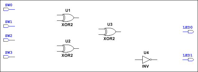
 in the PLD components toolbar to display the Select a Component (PLD Style) dialog box and select and place an XOR2 gate. .
 - Echo until you lot have placed a total of three XOR2 gates.
- Click
 in the PLD components toolbar to brandish the Select a Component (PLD Mode) dialog box and select and place an inverter. .
 - Adapt the components every bit shown below:
- Wire the PLD subcircuit as shown below:
- Relieve the PLD subcircuit.
- Render to the master design page and save the design.
The New Design dialog box displays.
A blank Multisim pattern file displays.
VCC is in the Sources group, POWER_SOURCES family.
J1 is DSWPK_4, constitute in the Basic group, SWITCH family unit.
The probes (PROBE_GREEN) are in the Indicators group, PROBE family.
The New PLD Design dialog box displays with NI Digital Electronics FPGA Board preselected.
The contents of the subcircuit display, with the port connectors LED0, LED1, SW0, SW1, SW2 and SW3.

This topic refers to education-specific features of Multisim.
Simulating the design
Complete the following steps to simulate your design.
- Beginning simulation and use J1 to specify four-bit words.
- Finish the simulation.
The circuit counts the number of HIGH inputs in the word and displays the result on the probes, ane for an ODD number of HIGH inputs and 1 for an EVEN number of High inputs.
4-Flake Parity Generator Truth Table:

This topic refers to teaching-specific features of Multisim.
Exporting the pattern
Complete the post-obit steps to export your blueprint to the NI Digital Electronics FPGA Board.
- Connect the NI Digital Electronics FPGA Board to your computer and switch it on.
- Open the PLD subcircuit in Multisim so that it is the active page.
- Select Transfer»Export to PLD.
- Select Program the connected PLD.
- Click Side by side.
- Under Xilinx tool, select the 64-chip version of your installed Xilinx tool, for example, Xilinx ISE Pattern Suite xiv.5.
- Click Refresh to bank check the connectedness.
- Click Stop.
- When the consign is completed:
- Toggle switches SW0 - SW3 on the Digital Electronics FPGA Board and compare the results to the 4-Bit Parity Generator Truth Table in step ane.
 This command is disabled if the active page is non a PLD design.
The PLD Export dialog box displays.
Step ii of the PLD Export dialog box displays.
If it is not in the list, manually select the directory it is installed in.
The Device Status dialog box displays. After a few seconds, the Device status changes to Detected.
 If the Device status changes to Non continued or drivers not installed, confirm that the 64-fleck version of a supported Xilinx tool is selected, the FPGA board is connected and switched on and yous have up-to-date drivers for the board. Click Refresh.
A PLD Export dialog box displays the status of the steps involved in the procedure. For example, Step 7 of 11: Map.
More than detailed messages, warnings, and any errors announced in the Results tab as the selected Xilinx tool programs the continued PLD. These letters are supplied from the Xilinx tool. For information about these, refer to the Xilinx assistance.
At the same time, an indicator consisting of moving zeros and ones appears below the hardware device target icon in the Design Toolbox.
If you cancel the PLD export, this indicator continues to motility until the current step is fully terminated.
If you lot click Hibernate, the PLD Export dialog box disappears, just the indicator continues to move until the export completes. To show the PLD Export dialog box again, select Transfer»View export progress.
This topic refers to teaching-specific features of Multisim.
WAS THIS Article HELPFUL?
blountsieneat1998.blogspot.com
Source: https://zone.ni.com/reference/en-XX/help/375482B-01/multisim/pldtutorial/
0 Response to "Can You Upload Plc Specs Into Multisim"
Post a Comment